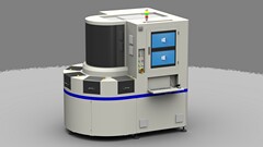
Wafer Appearance Inspection Machine Z21130

Device capabilities
⚪ Wafer class: Mini LED wafer, photosensitive diode.
⚪ Front: Electrode (defect, scratch/scratch, dirty, gold, bubbling, orientation) luminous zone (multi-cell, spalling, crystallite, edge collapse, deformation, residue) isolation groove (dirty, scratched, excessive, scratched, collapsed).
⚪ Reverse: poor cutting, concave and convex points, collapse, loss of crystals.
Product Highlights
⚪ With 3 magnification mirror groups, the user can choose the detection magnification for the grain or defect size, and the system has a minimum resolution of 0.5um, which can usually detect the defect size of about 1.5um.
⚪ Using advanced light imaging technology, combined with light and dark light field methods and light source angle, brightness and image taking mode, different types of defect imaging can be corresponded to.
⚪All inspection results are archived, providing defect source data to help analyze the benefits of production defects.